CHIP ON MODULE
ASSEMBLY
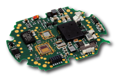
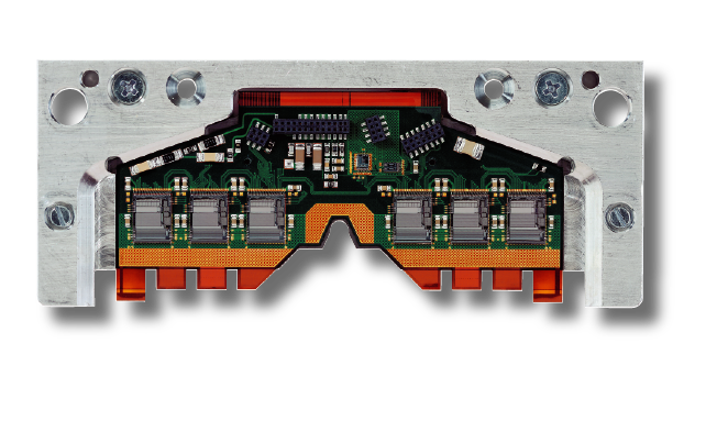
Depending on the application (eg. inside a contact lens!) achieving a minimum chip thickness is essential. HMT can handle the assembly of dice thinned (to 50µm).
About HiDensity Modules
Our business is miniature electronics. While the ultimate integration level is an integrated circuit, often the right miniaturisation for a product is a high density module or particularly a combination of integrated elements and miniature assembly. In offering both high density modules and full integration options, HMT can provide a complete solution with right split. Our specialities include:
- chip-on board (Au on Al wire-bonding), chip on chip
- flip-chip with solder balls, conductive and non-conductive epoxy, underfill and glob-top
- stud-bumping for flip-chip production of standard ICs in wafer form, including sawing, stocking
- multiple substrates down to 50µm thickness, including FR4, Rogers, Flex, ceramic and glass with smallest dimension PCB technologies, including filled microvias etc.
- component procurement and supplier management (ISO9001) for assemblers and components
- optical assembly in clean room & assembly of dice thinned (to 50um)
- smallest dimension PCB technologies, inc. 40µm track and clearance, down to 5µm Cu thickness and filled microvias with pad of 120µm and hole of 50µm.
- electrical module test design (hardware and software) and production test
HiDensity Substrates - PCB, FR4
| Parameter | Specification | Parameter | Specification |
|---|---|---|---|
| Double side | Both side are available for conductor layer, SMD, Flip-Chip or COB components | Conductors | Copper |
| Via’s | 200 μm typical, 25 μm (fine line), micro-vias (filled), staggered, stacked | Conductor resolution | 150 μm (typical), 50 μm (fine line) |
| Printed resistors | Based on polymer paste | Components | Flip-Chip, Chip on Board (COB), SMD down to 01005, Beam-Lead |
| Resistor tolerance | 30% un-trimmed, 2% trimmed | WireBonding | Gold 25, 30 μm, Aluminum 25, 33 μm |
| Resistor geometry | 0.5 x 0.5 mm (trimable), 0.2 x 0.2 mm | Ribbon Bonding | Gold up to 400 μm, Aluminum up to 400 μm |
| Resistor types | Linear, NTC, PTC | Outline | all forms (laser-cut, milling, cutting punch tooling) |
| Resistor trimming | active, passive | Connectors | SIL, DIL, Quad SMD and wire |
| Test | 100% |
Chip on Module Assembly
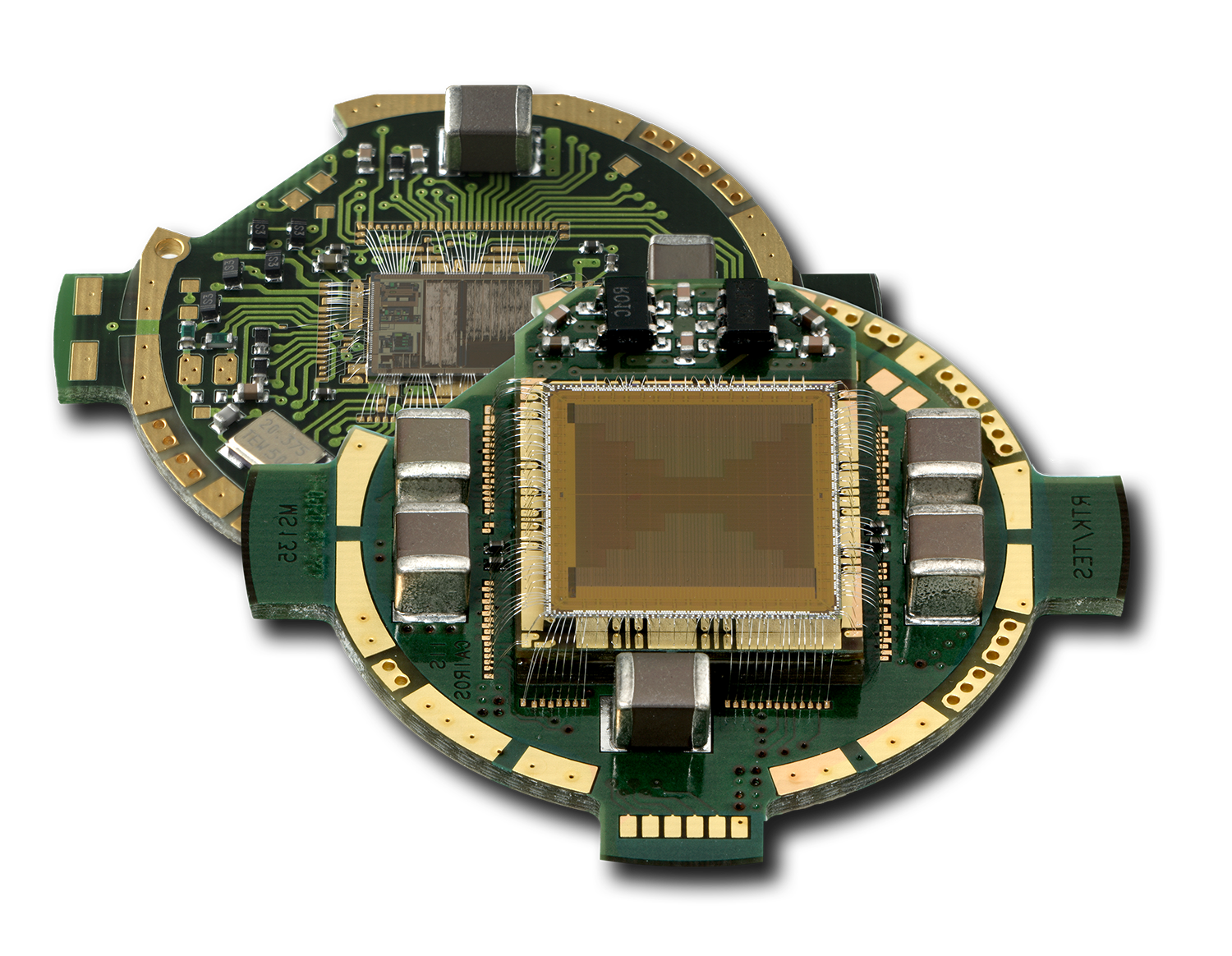
Bare dice and chip-scale packages can be mounted with the following techniques:
- chip on board (COB) with conductive or non-conductive die attach, wirebonding (Au/Al, wire or ribbon to flash gold on PCB) and glob-top
- chip-on-chip with wire-bonding from each chip to the board and between chips
- flip-chip with solder balls (min. pitch ca. 250µm), solder on copper pillar (min. pitch ca. 150µm), stud-bump with conductive or non-conductive adhesive, under-fill and glob-top
HMT can handle the use of purchased standard ICs in wafer form including thinning, sawing and stocking. Wafers can additionally be in-house stud-bumped where a post-processing solder ball deposition is not possible or not appropriate for the volumes.
Depending on the application (eg. inside a contact lens!) achieving a minimum chip thickness is essential. HMT can handle the assembly of dice thinned (to 50µm).